Jane Street: Really Low Latency Multipliers and Cryptographic Puzzles

At Jane Street, we have some experience using FPGAs for low-latency systems–FPGAs are programmable hardware where you get the speed of an application-specific integrated circuit (ASIC) but without being committed to a design that’s burned into the chip. It wasn’t so long ago that FPGAs were expensive and rare, but these days, you can rent a $5,000 card on the Amazon AWS cloud for less than $3 an hour.

Recently, my entry in a competition for a decades-old puzzle showed how clever use of FPGAs can be used to push the boundaries of low-latency computing.

Cryptographic puzzles

Back in 1999, MIT’s Computer Science and Artificial Intelligence Lab created a time capsule that included a cryptographic puzzle designed by Ron Rivest (the “R” in RSA). The puzzle was to calculate 22t (mod n) for t = 79,685,186,856,218 and a 2048-bit semiprime modulus n. (A semiprime is the result of multiplying two primes together.) The prompt helpfully pointed out that the problem could be solved by starting from 2 and repeatedly squaring t times mod n. For example (from the prompt):

Suppose n = 11*23 = 253, and t = 10.  Then we can compute:
	2^(2^1) = 2^2 = 4 (mod 253)
	2^(2^2) = 4^2 = 16 (mod 253)
	2^(2^3) = 16^2 = 3 (mod 253)
	2^(2^4) = 3^2 = 9 (mod 253)
	2^(2^5) = 9^2 = 81 (mod 253)
	2^(2^6) = 81^2 = 236 (mod 253)
	2^(2^7) = 236^2 = 36 (mod 253)
	2^(2^8) = 36^2 = 31 (mod 253)
	2^(2^9) = 31^2 = 202 (mod 253)
	w = 2^(2^t) = 2^(2^10) = 202^2 = 71 (mod 253)

Rivest’s team chose the number of squarings t so that, if Moore’s Law held up, the puzzle would take around 35 years to crack.

We can expect internal chip speeds to increase by a factor of approximately 13 overall up to 2012, when the clock rates reach about 10GHz. After that improvements seem more difficult, but we estimate that another factor of five might be achievable by 2034. Thus, the overall rate of computation should go through approximately six doublings by 2034.

But then in 2019 it was announced that Belgian programmer Bernard Fabrot had been able to crack the puzzle in just three and a half years, a decade and a half ahead of schedule. There were no magic tricks in his approach. It was just that Rivest’s original estimate was off by a factor of ten. While we don’t have 10GHz CPUs sitting in our desktops (mainly due to thermal issues), CPU and multi-core architecture has advanced dramatically. A few weeks after Bernard announced that he solved the puzzle, another group called Cryptophage announced they had, too, using FPGAs in just two months.

An interesting aspect of this puzzle is that while it’s expensive to compute, it’s cheap for the designer of the puzzle to verify the solution. That’s because if you know the two primes p and q that are the factors of n, you can use Euler’s totient function to calculate phi(n) = (p-1)(q-1). Once you have that, the large exponent can be reduced from 22t (mod n) to a much faster to calculate 22t (mod phi(n)) (mod n).

These types of cryptographic puzzles are part of a class of Verifiable Delay Functions (VDF): problems that take some medium to large quantity of non-parallelizable work to compute, but that can be verified quickly. They are useful in decentralized blockchain systems, for instance for randomness beacons, voting, and proofs of replication. While Rivest’s puzzle required secret knowledge to quickly verify the result, there are many proposed constructions that allow a VDF to be publicly verified without secret knowledge.

Using FPGAs for low latency

In late 2019, the VDF alliance began a competition to find the lowest latency achievable for a VDF problem similar to Ron Rivest’s 1999 puzzle. The idea was that by submitting such problems to fierce competition, you could help battle-test systems that rely on VDFs.

The competition required participants to solve a scaled-down version of the Rivest puzzle, with a t of ~233 instead of 246, and a 1024-bit modulus. Contestants were also given p in advance.

Ozturk multiplier

The winner from the first round of the VDF alliance competition was Eric Pearson, using an Ozturk multiplier architecture. This type of multiplier takes advantage of a couple of tricks that FPGAs can do extremely efficiently that GPUs or CPUs can’t:

  1. Redundant bit representation (RBR). This means your 1024-bit number is split into n equally-sized words (in this case n = 64 words, each 16 bits), but then each word gets an extra redundant bit. The advantage of this is when you accumulate all the partial products from a multiplication, you don’t need to propagate carry bits through the whole 2048-bit result–you only need to propagate it to the neighboring word. On an FPGA, the maximum speed your circuit can operate will be limited by the slowest path–which is often the carry chain. This helps makes the squaring part of the equation run as fast as possible. When we square, we use the same algorithm as multiplication, except half of the partial products are identical. We don’t need to calculate them twice: we just bit shift them by 1 bit, essentially doubling them for free.

  2. Modulo reduction using lookup tables. Every bit that is set past the 1024-bit modulo boundary can be precalculated as a modulo p value and added back onto the original result–e.g., 22000 becomes 22000 % p. This way, a 2048-bit result can be reduced back to a 1024 + log2(height of the pre-computed word tree) bit modulo p value. This takes a lot of memory on the FPGA, but allows you to calculate modulo p in just three clock cycles: two to look up RAM, one to fold the offsets back into the result. Both this technique and using RBR help speed up the final “modulo p” step required by the VDF equation.

Eric’s implementation took advantage of the LUT size in this generation of FPGA (6 input) to more efficiently map the memory reduction elements and compression trees in the multiplier partial product accumulation. For the modulo reduction, instead of block RAMs he used the faster LUTRAM, which further saves a clock cycle; taking this saved clock cycle to add more pipelining to paths where timing was critical allowed for an operating frequency of 158.6MHz (total 4-stage pipeline). This meant a single iteration of the VDF could be performed in 25.2ns. The design spanned most of the FPGA, crossed multiple super logic regions (abbreviated SLR, these are individual silicon dies that are used to form one large chip), and required power management to run. Eric commented in his submission that the FPGA actually burns as much as 48W when running in the AWS cloud.

Predictive Montgomery multiplier

There was a third and final round of the competition where more alternative approaches to the problem were encouraged–the Ozturk multiplier code was actually supplied in a basic form for the first rounds, so it was important to make sure there wasn’t some alternative design that might be faster than Ozturk. (Initially, no one wanted to spend the time trying to implement something from scratch only to find out it was not as good.) This sounded interesting to me so I came up with a novel “Predictive Montgomery multiplier” architecture which was the final round winner.

Tricks I used (again not efficiently possible on GPUs or CPUs):

  1. Montgomery multiplication with RBR. I decided to implement the modulo reduction scheme using Montgomery’s algorithm, which requires a transform into a Montgomery domain–but then modulo p becomes a fixed bit-shift which can be done on a FPGA in O(1) time. I only transform in and out of the Montgomery domain at the start and end of our 2n loops, so the overhead is not noticeable. I also modified the algorithm to work with RBR–this makes each individual step a little bit faster.

    Montgomery multiplication only involves multiplications, additions, and bit shifts–all of which are easy to implement in RBR, and will benefit from the shorter carry-chain. I also add an extra RBR word so that in total there are 65 words each of 17 bits to represent a 1024-bit number. This change allows a modification to the Montgomery algorithm so that it is guaranteed to produce a result less than p (a traditional Montgomery algorithm only brings the result to less than 2p). By using Montgomery multiplication I was able to save on a lot of FPGA area because the modulo step of the VDF equation becomes much easier.

  2. Log-3 compressor circuit with fast-carry. I decided to implement my multiplier as a simple cross-product multiplier using FPGA DSPs (digital signal processors, a small dedicated resource on the FPGA for performing multiplication efficiently). The chosen RBR bit width of 17 means one partial product only takes 1 DSP resource, followed by a final partial product accumulation stage using general FPGA LUTs. The maximum height of the tree used requires 128 columns, each containing 129 partial products, each 17 bits wide to be added together. I experimented with different log values and found folding the tree with arity 3, and using the FPGA adder fast-carry (rather than using compressor trees which did not utilize the fast-carry) gave the best results. This style of compressor implemented with RBR allowed me to squeeze even more performance out of the multiplier than before.

  3. Predictive branching. Montgomery multiplication requires a full 1024-bit squaring, followed by a 1024-bit multiplication where I only care about the lower 1024 bits of the result, followed by a 1024-bit multiplication, addition, and bit shift down (so I essentially only care about the upper 1024 bits of the result).

    The problem here is that a single SLR on the FPGA only has 2280 DSPs–and I really wanted to work in this budget, since communicating with multiple SLRs can make the whole design slower. A single squaring takes around 2120 DSPs, but a full multiplication will take 4225. To solve this problem I use predictive branching: the multiplier calculates partial products based on an inputs fed in via a crossbar, where the inputs are selected so I’m only calculating a full square, the lower 65 + x words, or the upper 65 + x words. Here x is the number of words past the boundary I calculate, to make sure I account for any carry overflow that might be getting erroneously included or discarded due to our RBR form.

    If I detect in the boundary words that might have this case (detected by all 1s and no free bits to absorb carry), I will branch and calculate the full 2048-bit (130-word) result, with the carry fully propagated. This is so rare that it hardly impacts performance, but this style of predictive branching allows us to implement the entire Montgomery RBR algorithm using a single SLR and 2272 DSPs. I also take advantage of the partial product tree and shortcut the extra addition in there without adding extra pipeline stages.

  4. Slower, shorter pipeline. Often, pipeline stages can be added to allow a design to achieve a higher frequency and higher throughput. But since this is for low latency, you actually don’t want to pipeline more than necessary–extra pipelines will increase the routing latency on signals in the FPGA as they now need to make “pit stops” to access the register. In my design, the main data path loop only has a single pipeline stage on the output of the predictive multiplier, which directly feeds back into the multiplier crossbar. This improvement not only helps improve latency, but also reduce the overall power used in the design. A slower clock means individual signals will be switching at a lower frequency, which leads to a quadratic reduction in power consumed on the FPGA.

My multiplier design ran at 65MHz and took 46ns (3 clock cycles) to finish one iteration of the VDF. It could be fully implemented on one SLR of the FPGA (a third of the FPGA, 2.3x less than the Ozturk design) and didn’t require any special power management as it consumed 3.7x less power (both designs were simulated in Vivado, FPGA design software). Because my design was smaller, it does lend itself to be scaled easier. If this design was scaled up (by using all 3 SLRs on the FPGA) to solve the original 35-year puzzle from Ron Rivest it would of taken us a little over two months!

The table below shows a comparison of the two 1024-bit architectures, with the ratio of improvement (so higher is better) shown in brackets where the Ozturk multiplier is the base 1.0x. My design had the lowest latency and won the round I was competing in, as well as a better power (in the table we show energy consumed as Joules per operation) and area efficiency compared to the Ozturk multiplier architecture. But overall Eric’s round 2 design was able to achieve a lower absolute latency.

Conclusion

All of this doesn’t connect directly to the work we do at Jane Street. In particular, we’re not likely to use VDFs in our infrastructure anytime soon. But the broad approach of using reconfigurable hardware to build solutions that can be orders of magnitude faster than what could be done in an ordinary CPU is at the core of what our group does. And, as this example highlights, building the most efficient solution requires you to think about completely new architectures, resource constraints, and capabilities than what you would ordinarily consider in software.

Notes

  1. There are other modulo reduction algorithms–for example Barret’s reduction and the Chinese remainder theorem, as well as other architectures that can be used for the actual underlying multiplier, such as Toom-Cook, Booth, and Karatsuba. I investigated all these approaches but found for various reasons that they didn’t map to this problem on a FPGA as well (i.e., Barret’s algorithm required subtractions which would make RBR more complicated and slower).

Open VDF: Partial Product Generation

In this blog we’ll look at partial product generation for the Öztürk multiplier. We’ve considered three techniques for partial product generation:

  1. Use small (17-bit) multipliers to generate partial products that feed into compressor trees. This was the approach used in the FPGA-based design leveraging the high speed DSPs.

  2. Use small (17-bit) multipliers as above, but using Booth encoding.

  3. Use bitwise partial product generation with AND gates.

The last approach is theoretically the best for ASIC designs from a complexity standpoint. However, since our goal is to achieve the lowest possible latency, we wanted to rule out the possibility that a more structured design, or an alternative encoding scheme, could end up producing a better result in practice.

As in the previous posts, we’ll take the approach of analyzing this discrete component of the design to guide our decisions on the best way to construct the full modular squaring unit. In this instance we will look at using multipliers and carry save adder trees to construct the squaring circuit.

Partial Product Generation

In our last post we introduced a large integer multiplier construction using the “schoolbook” approach. We reuse that concept here for partial product generation.

When using the polynomial multiplier design, one option is to divide the 2048 bit input into 16-bit digits. When using the redundant representation we arrive at 130 digits, each 17 bits in length. We can then multiply these 17-bit digits to form partial products, which are summed down the columns through the use of compressor trees.

An example is shown for squaring 4 digits in the following drawing. Recall that we can optimize for squaring by doubling (shifting left 1 bit) the duplicated partial products shown in light purple.

triangle.png

This approach works very well on FPGAs since it makes good use of the built in high-speed DSP blocks. On one popular FPGA platform, the DSPs support up to 26-bit by 17-bit multiplication.

For an ASIC we can break this down even further and consider each digit in the polynomial to be one bit wide. In this case, the schoolbook algorithm is the same, but partial product generation is reduced to a single AND gate per pair of terms. The result is many more partial products and therefore larger compressor trees to sum them.

In concrete terms, we found the bitwise squaring approach resulted in the deepest column with 1,224 entries to sum. Using a tree, and including the PPG AND gate, results in a depth of log₂(1224) + 1 = 12 levels in the critical path. In pseudo code, disregarding for now the single AND gate:

A = [ x0, x1, …, x1223] # 16-bit unsigned integers
sum = 0
for i in range(len(A)):
    sum = sum + A[i]

Alternatively, with 17-bit digits, the PPG multiplier has to sum 34 inputs and the compressor tree has to sum 130 partial products, leading to a total depth of log₂(34) + log₂(130) = 13 levels. In pseudo code:

Cn = An * Bn
sum = 0
for i in range(130):
    sum = sum + C[i]

In the following sections we present the results for these two approaches.

Booth Encoding

In addition to considering a standard representation multiplier we also considered a Booth encoded multiplier.

Booth’s multiplication algorithm was originally developed to perform signed multiplication. It can also have performance advantages, particularly when the operands contain consecutive ones or zeros. We won’t go into detail on the algorithm as there is abundant material online. Examples include Booth’s multiplication algorithm and Booth’s original paper on the topic.

Our purpose in exploring it here is to see if it offers any advantage for low latency designs.

Study Results

We considered four implementations for partial product generation:

  1. 17x17 bit multiplier PPG followed by compressors coded using “+”

  2. 17x17 bit Booth encoded multiplier PPG followed by compressors coded using “+”

  3. 17x17 bit Booth encoded multiplier PPG followed by compressors coded using explicit trees

  4. 1x1 bit PPG using AND gates followed by compressors coded using “+”. This design is architected specifically to minimize critical path gate depth for a low latency ASIC.

We will begin by first identifying the best approach to building a 17 bit x 17 bit multiplier (implementations #1 through #3), and then compare this result to a 1 bit x 1 bit PPG approaching using AND gates.

17 bit x 17 bit Multipliers

We first considered the 17x17 bit multiplier on its own by looking at three designs:

  1. 17x17 bit multiplier coded with “*”

  2. 17x17 bit Booth encoded multiplier coded with “+” for internal accumulators

  3. 17x17 bit Booth encoded multiplier coded with bit level compressors for internal accumulators

The multiplier results are shown in the following chart:

Comparison of 17x17 multiplier PPA vs. multiplier baseline coded using “*”

Comparison of 17x17 multiplier PPA vs. multiplier baseline coded using “*”

In this chart, latency refers to the lowest latency where timing closes. For area and power measurements each design style are measured at iso-latency for an aggressive latency target. Individual component sizes are chosen to be representative of what would be needed for a full 2048-bit modular squaring design.

From these results it is clear that “*” is the preferred approach for building a multiplier. This is the multiplier we will assume as we look at the full squaring operation in the next section.

PPG with AND gates vs. 17x17 Multipliers

For the entire squaring operation we took the best multiplier from above, paired it with a 130 element compressor, and then compared it to a single large compressor tree to assess the relative performance:

  1. 1224 element compressor tree coded with “+”

  2. 17x17 multiplier coded with “*”, followed by a 130 element compressor tree

PPA results are shown in the following chart:

PPG using 1224 element compressor tree vs a 17x17 multiplier plus 130 element compressor tree

PPG using 1224 element compressor tree vs a 17x17 multiplier plus 130 element compressor tree

Again we find that the simpler approach produces the best results, that is, it is better to build a single large compressor tree per polynomial digit rather than use a two level design that uses 17x17 bit multipliers.

These results align with those from our earlier CSA blog where we looked at composing large CSA trees from smaller component trees. At a high level, this is not surprising. We’ve essentially replaced some of the component trees from the earlier block with small multipliers, and as a results some of the same inefficiencies exist. Namely, the synthesis tool is no longer able to optimize over the entire tree. This means that most, or all, of the sub-components are suboptimal for the particular circumstances where they are instantiated.

Note that we did not take into account the required PPG AND gate. However, we expect it to be a small incremental cost and will confirm this when we look at the entire modular squaring unit.

Conclusions

In this blog we looked at using various styles of multipliers to generate partial products for the modular squaring operation. The results reinforce some of our conclusions from earlier blogs, specifically:

  • Explicitly using an alternative multiplier encoding style (Booth) produced worse results than letting the tools optimize

  • We consistently see that a simpler coding style for arithmetic operations (“+”, “*”) leads to better results when using modern ASIC EDA tools

The only remaining question before building the entire modular squaring unit is to consider what bitwidth size should be used for the polynomial coefficients. When designing for an FPGA we were constrained by the size of the available DSP resources. However, this is no longer the case on an ASIC where we’re free to build the components that we need. In the next blog we’ll discuss the tradeoffs involved in various bitwidth sizes, and perform an analysis to identify the optimal choice to take forward.

Source Code

Source code for the designs presented here are available on GitHub at supranational/hardware and is licensed under the Apache 2 license.

Acknowledgements

We’d like provide a special acknowledgement to Synopsys® for their support of this work.

Open VDF: Carry Save Adder

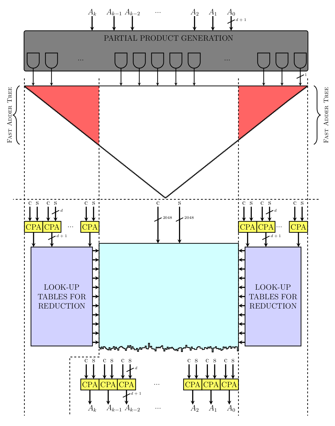
In this post we’ll look at the construction of low latency carry save adders (CSAs) and compressor trees for use in a low latency MSU. These structures comprise the bulk of the Öztürk design. In the architecture drawing below both the white and red upside down triangles and the turquoise rectangle are nearly 100% compressor trees, accounting for >80% of the logic in the design.

ozturk.png

Compressor Trees

Compressor trees perform the function of accumulating an array of numbers into a final redundant sum in a low latency manner. In our case the function we’re interested in is (in pseudo python):

A = [ x0, x1, …, xn] # x0 .. xn are 16-bit unsigned integers
sum = 0
for i in range(len(A)):
sum = sum + A[i]

Because we need low latency it is not sufficient to sum the values in series as implied by the code. This section will walk through the techniques needed to achieve low latency using compressors, trees, and redundant representation.

Bit-level compressors

At the lowest level a compressor takes as input a small number of input bits and sums them, producing a redundant carry and save output. Common compressor sizes are 3:2, 4:2, 7:3, and 9:4. The page ASIC Design for Signal Processing describes these bit level compressors in more detail. We combine these bit level compressors to form carry-save adders, which use a redundant representation to reduce the latency of adding 3 or more inputs.

Low latency adders

If you are not familiar with adders in general our previous blog post may be of interest. In that post we looked at the implementation of low latency adders and considered a variety of adder structures.

Recall that the key challenge with building low latency adder circuits is handling carries. The basic approach to adding two numbers is called a ripple carry adder and matches what you learned in school. Carries from one column are immediately propagated and summed into the next column. This creates a serial chain of carry dependencies as long as the width of the number, leading to high gate depth and slow circuits.

The following drawing shows a 4-bit ripple carry adder with a full adder depth of 4 (C1 through C4):

“4-bit ripple carry adder made up of four 1-bit full adders” by Cburnett (Own work) CC BY-SA 3.0

4-bit ripple carry adder made up of four 1-bit full adders” by Cburnett (Own work) CC BY-SA 3.0

Carry save adder: A carry save adder on the other hand breaks the carry chain by using bit level compressors to sum two numbers with no carry propagation. With this approach summing two numbers always has the same latency, regardless of the data width.

A 4-bit carry save adder has a full adder depth of 1 for any bitwidth, as shown:

One thing to take into account with carry-save adders is that they produce two outputs, carry and sum, instead of a single sum. Our final design compensates for this by using a carry propagate adder (CPA) to produce a single result, but we only need to do this once at the end rather than at every stage of the tree, a big latency saver.

Compressor trees

The Ozturk design requires accumulating large numbers of polynomial coefficients in both the squaring and reduction portions of the design. For a 2048 bit modulus and 16 bit coefficients we need to accumulate ~1200 16-bit multiplier partial products in the squaring portion of the design and ~1100 coefficients in the reduction portion of the design. If done serially using carry-save adders this would result in an adder depth of ~1200 and a very slow circuit.

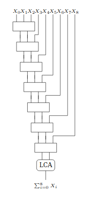
The following drawing shows an example for serially adding 8 inputs:


Instead we can take advantage of the commutative property of addition and structure these additions into a tree of log(n) depth, as shown below. In this case the levels of carry-save adders for 8 inputs drops to 4:


In this study we analyze the compressor trees required for the Ozturk design and begin to look at implications for the full MSU design.

Study Approach

For this study we chose sizes that correspond to the 2048-bit Öztürk design, but we expect the results are applicable to compressor trees in general.

The Intel white-paper Large Integer Squaring on Intel® Architecture Processors provides a good general background on large integer multiplication and squaring techniques. To illustrate with small numbers, suppose the task is to square a 4-digit number. The drawing below shows the schoolbook multiply adapted to a squaring operation.


triangle.png

First the partial products are generated by multiplying the individual digits together. Each result is inserted in the appropriate column, then the columns are summed (using compressor trees) to produce the product, which is twice as wide as the input. When squaring, the two operands are the same, therefore the light purple partial products will appear twice (for example x0*x1 and x1*x0). Rather than add them twice we optimize by generating these partial products once and then double the result, which is simply a 1 bit shift left in hardware.

In our case we assume 16-bit digits and 130 coefficients, leading to compressor trees of depth ~1200 in the middle columns. For reduction we have a nearly constant depth of around 1100 inputs, with some variation depending on the particular fixed modulus.

Given a compressor tree size we can then either consider it as a monolithic block or compose it from smaller building blocks. Functionally the approaches are the same but there are physical and tool implications, including:

  • The ability of the tools to optimize a design of the given size. Above a certain size and complexity runtimes become prohibitively long and the tools tend to do less well finding ideal implementations.

  • The power, performance, and area implications of replicating thousands of a small core design vs. optimizing individual columns specifically for the number of inputs they need to sum.

  • The opportunity to spend significant effort optimizing a single cell that is leveraged many times (perhaps using custom cells) vs. spreading that effort around.

In this case we consider 3 cases, a 1-level compressor design, as well as a 2 or 3-level balanced design. We use the term balanced tree to mean choosing a compressor size such that the number of inputs and therefore the latency consumed at each level are approximately equal. This leads to the following sized trees:

  • 1-level compressor: 1224-input x 17-bit

  • 2-level compressor: 72-input x 17-bit

  • 3-level compressor: 22-input x 17-bit

Impact of Performance on Power

Minimizing latency has a cascade of effects that result in large power increases. These come from insertion of more low voltage threshold (VT) devices, larger drive strength, higher voltage, and higher leakage. Specifically:

  • ULVT (ultra-low voltage threshold) devices replace LVT (low voltage threshold) and SVT (standard voltage threshold) devices in the critical path. ULVT devices transition faster at the expense of higher power and leakage.

  • Drive strength, which is the ability of gates and transistors to transmit current onto a wire, increases. This increases power and area.

  • Voltage is increased for higher performance, increasing power.

  • Higher voltage increases leakage current and leads to higher temperatures, which further increases leakage.

These factors mean that minimizing latency comes at a high cost in power and heat.

Study Results

Compressor Construction

To start we explored building compressor trees using a variety of bit level building blocks (compressors of size 3:2, 4:2, and 7:3) and tree styles (Wallace, Dadda). Like in the CPA study, these differences had little impact on the final outcome. By default the tools look through the hierarchy and apply transformations that reshape and improve the circuit. When the tools are forced to keep the structure intact the resulting circuit performance is somewhat worse.

We also compared these designs to simply using a series of “+” operations to sum many inputs. There are two big potential pitfalls with this approach:

  1. If the tools treat it as a long linear chain instead of forming it into a tree then latency would be very bad.

  2. If each “+” is implemented as a carry propagate adder then the carry chain latency would be very long, exactly the problem we hope to avoid by using carry save adders.

It turns out neither of these pitfalls occurs. When coded using “+” the tool is able to recognize the arithmetic function and apply specialized arithmetic optimizations that target low latency. Specifically, it creates a tree structure and uses carry save adders internal to the tree to keep latency low.

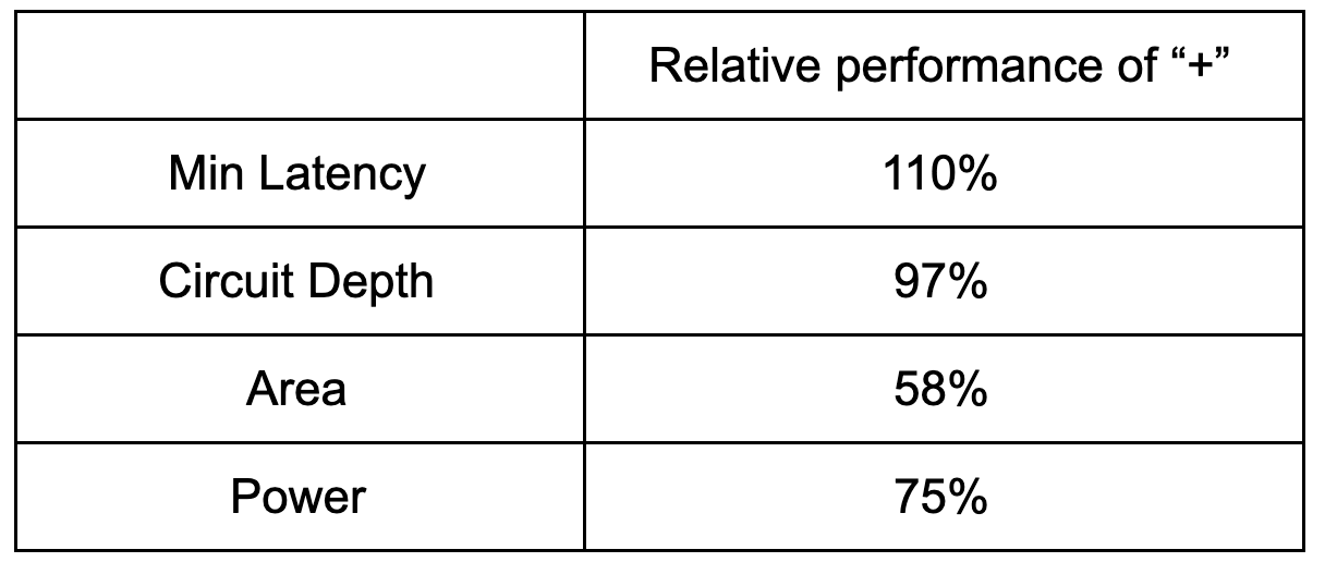
In the end, the results using an explicit tree and a series of “+” operations are shown in the table below:

result1.png

Relative performance of a compressor built with a “+” operations vs. an explicit tree structure with bit level compressor cells

As can be seen, the minimum achievable latency was slightly better using the bit level implementation, while the other metrics were worse. Given these similarity of the metrics and the simplicity of the “+” based approach, the “+” based approach is preferred. Interestingly, similar experiments with FPGA designs showed worse performance using the “+” approach vs. the bit level approach due to the heavy use of carry propagate adders.

Compressor Size and Number of Levels

Having determined the best way to code the compressor trees, we next looked at building a 1224-input compressor tree in 1, 2, and 3 levels. Our reasoning for trying a multi-level design was that smaller building block circuits might allow the tools to do a better job in optimizing this core component, which could then be repeatedly tiled.

The following table shows the results for the various trees at the lowest achievable latency. Latency, area, and power are relative to a 1-level design baseline, and encompass the compressor trees needed for both the squaring and reduction parts of the design. The instance count shows the estimated number of trees required in a full 2048-bit square-reduce design.

result 2.png

And in chart form:

result3.png

The 1-level design is clearly better for latency and power. Area is slightly worse for the 1-level design, but this is not a big concern as the incremental silicon cost is a marginal price to pay for improved power and performance.

Building on the themes from this and the previous blog, we believe the 1-level design does better because the tools are able to optimize for the entire circuit. In constructing larger trees from smaller components, each of the smaller components has a critical path driven by the low latency cells. This critical path is built with low voltage threshold cells with larger drive strengths in order to meet timing. However, once tiled together into larger trees, most of these paths are no longer critical in the larger circuit, meaning that the increased performance and power goes to waste. Further, the actual critical path of the larger circuit may not fully align with the fastest paths in the smaller components, resulting in a longer latency.

These results point us in the direction of focusing on the 1-level compressor tree design rather than a multi-level design, thereby giving the tools the most opportunity to optimize.

Conclusions

  • In general special care is not needed to build low latency compressor trees for ASICs — “+” is sufficient. The tools are very good.

  • A 1-level tree design is preferred over a 2 or 3-level design.

  • It is preferable to synthesize each compressor tree for the exact number of inputs needed rather than tiling out a larger tree from smaller components. This results in significant area and power savings.

Source Code

Source code for the designs presented here are available on GitHub at supranational/hardware and is licensed under the Apache 2 license.

Acknowledgements

We’d like provide a special acknowledgement to Synopsys® for their support of this work.

Open VDF: Carry Propagate Adders

Adders play an important role in any multiplier design, including the Öztürk design. There are two types of adders used in the design:

  • Carry Propagate Adders (CPAs) take some number of inputs and compute a sum by fully propagating the carries. The adders taught in elementary school fall into this category. Wikipedia provides a nice overview.

  • Carry Save Adders (CSAs) take some number of inputs and produce two redundant outputs, sum and carry. Producing two outputs means the carries do not have to be propagated, an important latency consideration. Wikipedia also provides an overview of these.

CPAs are used sparingly in the Öztürk design to minimize latency but do show up in two places (yellow boxes), at the bottom of both large CSA trees (red triangles). In both cases they are used to reduce the carry and sum the outputs of the CSA trees into a single value that can be used for reduction and squaring. The white portion of the squaring CSA can produce a result in carry/sum form that flows straight into the reduction CSA, without any CPA needed.

ozturk design.png

In this post we’ll look at the construction of low latency carry propagate adders. These have been well studied in the past but we wanted to have a fresh look for a couple of reasons.

  • Our target of lowest latency possible is pretty unusual in the silicon industry. Typically designs target a balance of latency and throughput.

  • It’s difficult to find published work based on recent process technology. We hope to fill some of that gap in this blog.

The data for this and subsequent posts is derived from synthesis runs using modern tools and processes.

Carry Propagate Adders

A key challenge with building low latency adder circuits is handling carries. The basic approach to adding two numbers is called a ripple carry adder and matches what was taught in high school. Carries from one column are immediately propagated and summed into the next column. This creates a serial chain of carry dependency as long as the width of the number, leading to high gate depth and high latency circuits.

The following drawing shows a 4-bit ripple carry adder with a full adder depth of 4:

“4-bit ripple carry adder made up of four 1-bit full adders” by Cburnett (Own work) CC BY-SA 3.0

4-bit ripple carry adder made up of four 1-bit full adders” by Cburnett (Own work) CC BY-SA 3.0

You can also watch an animation of a ripple carry adder in action.

Fortunately there are techniques to reduce the gate depth at the cost of additional logic. We implemented several parallel prefix adders, which are a form of carry lookahead adder, and explored their use in this design. Some references to consult for more detail are the slide set by Kostas Vitrooulis and the paper “A Taxonomy of Parallel Prefix Networks” by David Harris.

In this study we’ll compare the performance of adders consisting of ripple carry, Brent Kung, Kogge Stone, and “+” (i.e. write “a + b” and leave it to the tool to figure out).

Optimization Goals — Power, Performance, Area (PPA)

The main metrics to consider are power (watts), performance (ns latency), and area (mm²).

Theoretically we would expect to see something along these lines:

  • Ripple carry — slow (long carry chain), low area (minimal replicated hardware), lower power due to less hardware

  • Brent Kung, Kogge Stone — fast, higher area (replicated logic to compute carry), higher power

  • + — unknown, dependent on what the tool does

The following data is all presented in relative terms using a 16-bit adder as the test case. We use “+” as a baseline (1.0) and compare the relative performance of the other implementations.

PPA Measurements

  • Performance: Performance for VDF evaluation is improved by reducing the time time it takes to perform a modular squaring, often measured in nanoseconds. To evaluate the lowest latency for different adder designs we swept a range of clock periods and looked for the shortest period with no negative slack, i.e. that met the timing goal. What we found is that in spite of significant differences in tree depth as coded in RTL, the results were all within the margin of error. The synthesis tool did a good job of taking apart the function and optimizing it to meet design targets.

  • Power: In fact, we saw similar results for power…

  • Area: and area.

What uniform results! In all cases the design was transformed by the tool into a circuit that would meet the constraints. These results indicate there is little reason to use anything other than “+” to build adders. In fact, “letting the tool do its job” will be a common theme as we go forward.

A Retrospective

The tools have not always been this clever and historically would benefit from some implementation guidance. As an example here are results for a ripple carry adder with the latest generation of optimizations disabled. You can see it built a nice small, low power adder but was not able to transform it into a low latency adder.

Power and Performance

One interesting thing from the previous graph is that the relationship between power and latency is non-linear. In that case, latency increases by 2.3x while power decreases by 5x.

In the following graph we sweep latency and look at the resulting power compared to a target (100% latency). You can see that as latency goes down power rises and eventually hits a knee where it rises very steeply. As latency drops below 40% the tool is no longer able to meet the target (i.e. there is negative slack) and the power climbs a little less steeply.

power v performance.png

Conclusions and Code:

A few points to take away as we wrap up this post:

  • In general special care is not needed to build small low latency adders — “+” is sufficient.

  • The latest generation of tools is very good at optimizing and refactoring logic. It’s better to let them do the work.

  • Power increases quickly as latency decreases. This is not a surprise as the high performance chip industry (CPUs, GPUs, etc.) has been heavily focused on power for about two decades. Power will play a big role in this design too as we push for the lowest possible latency.

Upcoming Posts

In the upcoming posts we will dive into more detail on designing a low latency MSU by exploring:

  • Carry save adders (CSA) and compressor trees

  • Partial product generation (PPG)

  • Ideal coefficient bitwidth

  • Complete MSU design

Source Code

Source code for the designs presented here are available on GitHub at supranational/hardware and is licensed under the Apache 2 license.

Acknowledgements

We’d like provide a special acknowledgement to ePIC Blockchain for their feedback on implementing high performance CPAs and to Synopsys® and Dolphin Technology for their support of this work.

Open VDF: Öztürk Multiplier Design Overview

0_6AayQsff3TdL7JgF.png

Design Features

The current architecture under consideration is based on the Öztürk multiplier, which was presented in this MIT VDF Day talk. This design includes several features that are critical to a low latency hardware implementation.

  • Redundant polynomial representation — Eliminates the need to propagate a carry across 2k bits. A 2k carry would result in a very deep gate depth and slow design. Instead our longest carry is across a single digit and can be varied by choosing different digit sizes. In general carry propagation is a big challenge for low latency.

  • Fully unrolled pipeline — A typical traditional throughput oriented design uses pipelining to share resources and reduce area and power. In contrast this design stamps out enough hardware to eliminate sharing and extract all available parallelism. While resource sharing is not required, the design can be pipelined if desired.

  • Log depth compressor trees — Summing of partial products and reduction values comprises the bulk of the hardware. The design makes use of adder trees, resulting in a gate depth that is O(log n) with the number of inputs to sum.

  • Fixed modulus — With a fixed modulus the lookup tables are constants. We use 1-bit lookup tables, which means for each bit above 2k we’re choosing either the constant reduction value or zero to send to the compression trees. Zeros in the precomputed reduction values will be eliminated by the synthesis tool through constant propagation. In the end the reduction tables get absorbed into the reduction compression trees.

  • Critical path optimization — One clever optimization is to reduce from both the top and the bottom simultaneously, as opposed to from the top (Barrett) or bottom (Montgomery) alone. In doing so we can take advantage of the squarer triangle shape. The shallow portions needed for reduction (red) need to be fast to generate the reduction values and drive the reduction compression tree. The deepest portion of the triangle white can also be the slowest, since that result can intercept the end of the reduction compression tree. This reduces the overall critical path depth for the design and saves area and power.

Redundant Polynomial Representation Explained

The MSU architecture is optimized for a repeated-squaring setting. A novel redundant representation is utilized to achieve extremely low latency per modular squaring operation.

For efficiency of modular squaring operations, we utilize two levels of redundancy:

  • Each coefficient holds one extra bit to hold the extra carry bit resulting from coefficient-wise additions. This way, carry propagation is contained within each coefficient.

  • Each polynomial representing an integer holds an extra coefficient to reduce levels of reduction. The reduction operation consists of accumulating ~1024 2048-bit numbers together, producing a 2048+11 bit result. Instead of adding a second level of reduction to reduce these extra 11 bits, we utilize an extra redundant coefficient. This extra coefficient has negligible effect on the complexity of squaring and reduction operations, and the result of the reduction operation is still contained within 2048+11 bits.

As stated, the purpose of the redundant representation is to break the carry chain. Typically a squarer would have to propagate carries across the entire bit width being squared, resulting in a very deep critical path and long latency. In this design we break the carry chain at polynomial coefficient boundaries, resulting in a longest carry chain in the 20’s of bits.

Upcoming Posts

In the upcoming posts we will dive into more detail on designing a low latency MSU by exploring:

  • Carry propagate adders (CPA)

  • Carry save adders (CSA) and compressor trees

  • Partial product generation (PPG)

  • Ideal coefficient bitwidth

  • Complete MSU design

Source Code

Source code for the designs presented here are available on GitHub at supranational/hardware and is licensed under the Apache 2 license.

Open VDF: ASIC Introduction

synthesis.png

Welcome to the first in a series of posts about the design and implementation of a custom ASIC for computing verifiable delay functions, or VDFs. This post will provide a brief overview of VDFs, discuss the goals of the VDF hardware project, and lay out the foundations of the current design.

About VDFs

A verifiable delay function (VDF) is a cryptographic primitive that yields cryptographically verifiable time delays through sequential computation. One of the use cases of VDFs is generating public and unbiasable randomness without a trusted third party. This randomness can be used to enable more secure and scalable consensus protocols, make proofs-of-replication more efficient, and more. VDFs were first defined in a June 2018 paper by Stanford professor of cryptography Dan Boneh and others. Verifiable delay functions are defined as functions which require lots of sequential computation to evaluate, and for which the function output can be quickly verified via a short proof. An older ‘timelock puzzle’ construction by Rivest, Shamir and Wagner also uses sequential computation to create time delays and encrypt data ‘into the future’. In these RSA-based ‘timelock’ schemes, the sequential computation that must be done is modular squaring. More information about VDFs can be found at https://vdfresearch.org/.

Open VDF Project Goals

This project, as part of the VDF Alliance, began in early 2019 to evaluate the feasibility of developing fast, open, hardware for computing verifiable delay functions. While open source software powers so much of our core internet security today, open source hardware is still a nascent ecosystem, and open source hardware built for cryptography is even more niche. The goal of the Open VDF project is to provide some common building blocks for future cryptographic accelerators, share information about hardware design, and advance the state of the art for hardware acceleration of VDFs. Source code, as well as performance results from synthesis or other sources, will be shared where possible. We welcome and encourage feedback and participation from the community on improving the design and advancing the project forward.

Design Targets

Before discussing the current Open VDF design, it is important to understand the design goals of the custom hardware. Efficient computation of VDFs requires low latency modular squaring to evaluate the delay function and high throughput modular multiplication to generate the delay function proof. This initial blog series will focus solely on the low latency modular squaring. Lowering the latency of the VDF evaluation to approach its assumed minimum speed allows for improved user experience and security when used in blockchain protocols. This gap between the current state of the art hardware and the assumed lower bound is known as amax. In addition to being ‘fast’, the VDF processor must also be practical and affordable for home users.

Current Design

The current architecture under consideration is based on the Öztürk multiplier, which was presented in this MIT VDF Day talk. This modular squaring unit (MSU) is composed of two main operations:

  • Squaring: The design uses a schoolbook polynomial multiplication method to generate the square. There are many existing resources for learning more about this method, including here and also algorithm 7 here.

  • Reduction: We utilize a look-up table based reduction algorithm as explained in Algorithms 8 and 9 from. For our design, instead of a d-bit look-up table, we utilize a 1-bit look-up table approach. Also, for a more balanced critical path, instead of reducing the top ~2048 bits of the squaring operation, we reduce the most significant ~1024 bits and least significant ~1024 bits using out look-up table based approach, utilizing Montgomery Reduction for the least significant bits.

The data flows from top to bottom in this drawing through the following steps:

  • Partial product generation — In binary representation the partial products are formed by AND’ing the input coefficients according to the schoolbook squaring algorithm.

  • Partial product accumulation — The green, white and red triangles represent compressor trees (CSAs) that accumulate the partial products. The red triangles need to be as fast as possible to feed into reduction below. The middle white portion can take more time as it only feeds into the final output, keeping it out of the critical path.

  • Carry propagate adder (CPA) — Sums the carry and sum redundant outputs of the compressor trees into a single result.

  • Reduction lookup table reads — After squaring the resulting ~4k bits wide product needs to be reduced back to 2k bits. Precomputed reduction tables are indexed using the top 1k bits and bottom 1k bits, each producing a 2048 bit value. This results in ~2k polynomials that need to be summed with the output of the white portion of the triangle to produce a result in redundant form.

  • Reduction compression trees (turquoise box) — Since we are summing many partial products together the resulting polynomial coefficients will grow in width, up to about 29 bits.

  • CPA — Sums the carry and sum outputs of the reduction compression trees and partially reduces the wide coefficients from the previous step by carrying bits above bit 16 into the coefficient one degree higher.

Upcoming Posts

In the upcoming posts we will dive into more detail on designing a low latency MSU by exploring:

  • Öztürk multiplier design

  • Carry propagate adders (CPA)

  • Carry save adders (CSA) and compressor trees

  • Partial product generation (PPG)

  • Ideal coefficient bitwidth

  • Complete MSU design

Source Code

Source code for the designs presented here are available on GitHub at supranational/hardware and is licensed under the Apache 2 license.

VDF Alliance FPGA Competition Round 1 Results and Announcements

Competition Round 1 Results

On August 1st, the VDF Alliance launched a $100,000 competition to improve the security and scalability of blockchains through open source, high-performance hardware. Today we are excited to announce the results of the competition’s first round winner. Congratulations and thank you to Eric Pearson who was able to achieve a 78% increase in throughput over the baseline design! For his winning submission Eric was awarded $64,200, and his winning submission can be found here. We’d also like to thank everyone who submitted an entry in the first round of the competition. As a reward for your hard work we will be awarding $1,000 to each of the teams who submitted an entry but did not place first. Finally, we would like to thank our corporate partners, AWS, Synopsys, and Xilinx for their support of the competition and its logistics.

Competition Round 2 Launch

With Round 1 complete, Round 2 of the FPGA competition is officially underway. For the second round of the competition we are increasing the rewards from $3,000 to $5,000 per nanosecond reduction. In addition, we have also reset the prize pool back to a $100,000 maximum payout. The second round of the competition will end on December 30, 2019. For more information about the second round, please visit the VDF Alliance wiki.

New Prizes Announced

Today we are announcing two new $5,000 prizes focused on alternative approaches to low latency modular squaring for RSA VDFs. These two new competitions will end on January 30, 2020.

  • Prize #1 - Fastest Alternative FPGA Implementation: $5,000 will be awarded to the fastest VDF implementation on FPGA that uses an alternative approach than the ‘Ozturk’ algorithm. Potential algorithmic approaches include Montgomery, Barrett, and CRT.

  • Prize #2 - Best Research Paper on Low-Latency VDF Algorithms: $5,000 will be awarded to the research paper that describes the most promising and novel algorithm for a low latency RSA VDF. Best paper will be determined by a panel of judges and will be assessed on the novelty of approach, contribution to state of the art, and suitability for low latency ASIC implementation.

For the official rules on these prizes please see the wiki and feel free to reach out to hello@vdfalliance.org with any questions.

Get Involved!

The VDF Alliance is a collection of individuals, non-profits, academic institutions, and corporate partners building open source hardware for the blockchain ecosystem. If you are interested in participating please feel free to reach out to us by e-mail or on Telegram. If you are interested in learning more about our research and goals, please see VDFResearch.org, VDFAlliance.org, and the VDF Alliance wiki.


VDF Alliance Announces $100,000 FPGA Competition

The problem: Given 1024-bit input x, compute the verifiable delay function ‘h=x^(2^t) mod N’ as fast as possible.

t=2^30

N=12406669568412474139879892740481443274469842712573568412813185506497689533
7309138910015071214657674309443149407457493434579063840841220334555160125016
3310409336906745695712173376302391915172057213101976083872398463643608502208
9677296497856968322944926681990341411705803010652807392863301711868982662559
4484331

The prize: $100,000.

If that all makes sense, then what are we reading this for? Get to work.

If not, a bit of background on a competition about to kickoff that could change not just the face of blockchain technologies, but also how we go about designing and building hardware. It starts with Justin Drake, a researcher with the Ethereum Foundation, and one of the crypto world’s leading champions of the Verifiable Delay Function, or VDF (and then you can get to work).

VDFs are a low-level building block in cryptography, barely more than a year old. It’s the “V” or ‘verifiable’ in VDF that makes the approach so unique, says Drake dialing in from Croatia, at one of yet another gathering of the cryptographic faithful that keeps him in a constant state of motion around the globe. “It’s trustless,” Drake says, and “ for the first time, it adds this notion of time with which you can build all these cool things.”

One of those cool things is an unbiased proof of randomness. The “D” part of VDF, might be thought of as “difficulty” some amount of sequential computation (or delay element) that can produce a stream of random numbers that are very hard to stop. That difficulty, which results in a delay, prevents malicious actors from front-running the output of the pseudorandom generator (which is not so random or trustless). Add into that a lightweight auxiliary proof to verify those unbiased random numbers, and you have something perfect for the blockchain world. “It’s a way of sampling a block proposer to extend the blockchain,” Drake says. “It moves us from proof of work (the approach when verifying blocks today), to proof of stake.”

This proof of stake approach also moves much of the heavy lifting when extending the blockchain from software to more efficient hardware, a shift, assuming it’s successful, that has the potential to reduce the cost of extending the blockchain — all that crypto mining to solve  — by a factor of 10X or more.

“The Ethereum ecosystem alone currently uses on the order of 850 megawatts to extend blocks. That’s about $460 million in running costs per year,” says Tim Boeckmann, who promotes developing technologies for the AWS startup team from the United Kingdom. “With VDFs in Ethereum, there is an opportunity to bring down that cost to less than $0.13 million for the 0.25 megawatts of energy to power the hardware random beacons. Other blockchain protocols including Filecoin and Tezos are exploring this too. If we can help lower the amount of the world’s resources we use to bring blockchain technologies to more applications, why wouldn’t we?”

For starters, because it is hard. But the efforts of people like Simon Peffers, a former Intel engineer veteran chip designer, and the founder of Boston-based startup Supranational, offers reason to believe that we, and VDFs, can get there. Using a Field Programmable Gate Array (FPGA) running on AWS — the Amazon EC2 F1 instances — Peffers was able to solve the LCS35 Time Capsule Crypto-Puzzle, a cryptographic challenge put forth by MIT’s Laboratory for Computer Science in just two months.

If that sounds like a long time, the challenge, which debuted in 1999, was supposed to take 35 years of sequential computing to crack. Peffers was actually beat to the punch of solving the MIT puzzle by a Belgian coder, who used another method to solve the problem over the course of three-and-a-half years and arrived at the correct solution weeks before Peffers.

The time lock puzzle had some of the same elements as a VDF — the delay function that came with imposing sequential computing on the problem. For Peffers attacking the MIT competition boiled down to squaring a number nearly 80 trillion times, an operation that was designed to take decades even accounting for Moore’s Law. Peffers was able to do it in two months because of a well-designed algorithm running on a superfast FPGA, not to mention his more than two decades of chip design smarts.

But the point for Peffers was that well designed hardware in combination with smart algorithms was the key, and could also hold the key to taking VDFs and blockchain technologies mainstream.

“The biggest challenges for blockchain technology today are scalability and privacy,” Peffers says. “While the cryptographic community has made some outstanding developments that address these problems, many aren’t computationally practical. Hardware acceleration can improve the performance and cost of these algorithms ten, or even a hundred-fold, enabling them to be deployed, and used, on a day-to-day basis.”

Which gets us back to: Given 1024-bit input x, compute the VDF ‘h=x^(2^t) mod N’ as fast as possible. And $100,000 as an incentive to get it right.

Let the competition begin!

Beginning August 1, 2019, the Ethereum Foundation, the Interchain Foundation, Protocol Labs, Supranational, Synopsys, and Xilinx, with support from AWS, are sponsoring a $100,000 competition. The first round of the competition will run through the end of September, and will award a prize to the fastest FPGA design that solves the problem above. The primary infrastructure for the contest will be Amazon EC2 F1 instances.

  • In the first round of the competition participants will be awarded $3,000 per nanosecond that they reduce the speed of the FPGA baseline (initially set at 50ns per modular squaring).

  • The second round of the competition will begin around late October with details to follow after the conclusion of the first round.

  • At the completion of the first round, all competition submissions will be open sourced.This will encourage collaboration and sharing of results. Teamwork and collaboration is encouraged.

“It’s a new way of designing hardware, of open-sourcing it,” Drake says. “It’s something that has never been tried. Hopefully, it will not only push forward a culture of collaboration between all kinds of blockchain projects, but open up the hardware design industry as well.”

Drake imagines the winning teams will require a mix of skills. “You are going to need people who are really good at hardware design, but also people with algorithmic skills,” Drake says. “My guess is the winning team will have a combination of that expertise.”

So get on it. Hardware, glory, cash, and the key to randomness await.

For more contest details ,and to enter, go here: https://vdfalliance.org/contest

And more to get you pumped for the contest and VDFs

Amazon Web Services: “The VDF initiative will help the blockchain community improve the scalability of public blockchains, without compromising security. AWS sees this as an important opportunity to bring together builders and innovators, to collaborate on open source hardware design and democratize access to the tools needed for adopting blockchain technologies.” Tim Boeckmann, Emerging Technology Startup Business Development at AWS

Ethereum Foundation: “Verifiable delay functions uniquely tie physical time and cryptography into a promising new tool for the blockchain industry. The Ethereum Foundation is thrilled by the collaborative thrust to deploy public good VDF infrastructure around open hardware.” Justin Drake, Researcher at the Ethereum Foundation

Interchain Foundation: “VDFs are an exciting new cryptographic primitive with a number of important applications in blockchain security, scalability, and utility. We hope the collaborative effort to develop open source VDF hardware will inspire more general advancements in open source hardware development, which will be critical to the future of secure, decentralized computing.” Ethan Buchman, Technical Director at Interchain Foundation and co-founder of the Cosmos and Tendermint projects

Protocol Labs: “VDFs enable reliable timing across a trustless network, assuming all participants can execute them at comparable speeds. Collaboratively developing fast, open VDF hardware makes it harder for individuals to leverage proprietary designs to gain an unfair advantage.”

Supranational: “We’re thrilled to help advance the security and scalability of blockchain protocols through this collaboration. We hope VDFs are just the start of a new era in open source hardware for the blockchain ecosystem.” Sean Gulley, Chief Technology Officer at Supranational.

Synopsys: “A fast Verifiable Delay function (VDF) design is essential to improving the security of blockchain networks.  Low latency, high frequency, and stringent power requirements, on a large arithmetic function, make VDF a complex compute hardware that requires state of the art technology to design and validate the hardware in the shortest period of time. Synopsys technology and products are best in addressing these challenges, fully cloud-scalable on AWS, and hence are in the best position to support this unique contest.” Michael Sanie, VP marketing and strategy in the Design Group at Synopsys.

Xilinx: “Orders of magnitude performance and efficiency gains are achievable when developers have access to configuring and optimizing both hardware and software architectures. We are excited to see the results of this competition and how our adaptable compute platform will be harnessed to solve this challenging compute problem.” Vinay Singh, Sr. Director of Market Development, Xilinx

VDF Alliance Featured in Wired Magazine

Excerpt from: Wired Magazine

Although Fabrot didn’t know it, a group of computer scientists and cryptography experts were working on a project called Cryptophage, which was using specialized hardware meant specifically to solve the MIT puzzle.

Led by former Intel engineer Simon Peffers, the Cryptophage group was researching verifiable delay functions as a possible security mechanism for blockchains like Ethereum. Verifiable delay functions are a modern take on Rivest’s early work on time-delayed cryptography, and their solution can be derived only through sequential operations. In the course of their research, Peffers says, the Cryptophage group came across Rivest’s puzzle, which seemed like a good way to put their research to the test.

In mid-March, the group began to run an algorithm designed by Erdinc Ozturk, a researcher at Sabanci University, that was optimized to reduce the amount of delay between squaring operations. This algorithm was implemented on a field-programmable gate array, a multipurpose chip that is programmed to run only a specific algorithm, which makes it more efficient than a general-purpose CPU. Using Ozturk’s algorithm, this FPGA was about 10 times faster than a high-end commercial CPU running non-optimized software.

Based on the chip’s computing efficiency, the Cryptophage group calculated that they would have the correct solution to the MIT puzzle on the evening of May 10, just two months after they started the calculation. Yet when they reached out to MIT to let them know a solution was imminent, Rivest informed them that Fabrot had beaten them to the punch.

“We didn't have anyone come to us until these two came up to us on practically the same day to say 'we've solved your problem,'” Rivest says. “That's an astonishing coincidence.”

Rivest is quick to admit that he had overestimated the difficulty of his puzzle. Making predictions about improvements in technology is difficult on that long of a timescale, and Rivest says he didn’t anticipate breakthroughs like FPGA chips, which weren’t as sophisticated or widely available as they are today.

Although the Cryptophage group wasn’t the first to solve the puzzle, Peffers said they will still be at the ceremony to open the time capsule on May 15. Only the capsule’s designers know its full contents, though it does include contributions from Tim Berners-Lee, inventor of the World Wide Web; Bob Metcalfe, who invented ethernet; and Bill Gates, who contributed the original version of Altair BASIC, Microsoft’s first product. Fabrot said he is most excited to see an original copy of one of the earliest PC games, Zork, included in the capsule.”

For the full article see: https://www.wired.com/story/a-programmer-solved-a-20-year-old-forgotten-crypto-puzzle/

VDF Alliance Solves 20-Year-Old MIT Puzzle

This week MIT’s Computer Science and Artificial Intelligence Laboratory (CSAIL) announced that a 20-year-old cryptographic puzzle was just solved by a self-taught programmer from Belgium, 15 years earlier than MIT scientists expected.

Bernard Fabrot spent the last three and a half years computing the solution to a puzzle first announced by MIT researchers in 1999. Separately, another team led by tech executive Simon Peffers is nearing completion of computing a solution.

The puzzle essentially involves doing roughly 80 trillion successive squarings of a starting number, and was specifically designed to foil anyone trying to solve it more quickly by using parallel computing.

Fabrot and Peffers took very different approaches to the puzzle. Fabrot used a simple Intel Core i7-6700 found in consumer PCs, and computed the solution using the GNU Multiple Precision Arithmetic Library (GMP). Meanwhile, Peffers' team used a novel squaring algorithm (designed by Erdinç Öztürk from Sabanci University) to run on a programmable hardware accelerator called an FPGA. The team, which is working as part of a collaboration called Cryptophage, is on track to finish the puzzle on May 11 after only two months of computation.

“There have been hardware and software advances beyond what I predicted in 1999,” says MIT professor Ron Rivest, who first announced the puzzle in April 1999 tied to a celebration of 35 years of research at MIT’s Laboratory for Computer Science (now CSAIL). “The puzzle’s fundamental challenge of doing roughly 80 trillion squarings remains unbroken, but the resources required to do a single squaring have been reduced by much more than I predicted.”

The puzzle is an example of a “verifiable delay function” (VDF), meaning that its answer can only be solved after a certain number of steps. Because VDFs can also be used to create unbiased randomness, they’ve been proposed as potential approaches to improve the security and scalability of blockchain systems like Ethereum and Filecoin. 

In the original announcement, LCS promised that, if a correct solution was uncovered, they would open a special “time capsule” designed by architect Frank Gehry and filled with historical artifacts from the likes of Web inventor Tim Berners-Lee, Ethernet co-inventor Bob Metcalfe, and Microsoft founder Bill Gates. (Gates donated the original Altair BASIC that represented Microsoft’s first-ever product, which they developed for MITS in 1975.)

The capsule ceremony will happen Wednesday, May 15 at 4 p.m. at MIT’s Stata Center.